
Search This Supplers Products:Power AdapterLED Power SupplyPower AdapterBattery ChargerMedical Power SupplySwitching Power Supply
US Oregon certified power adapter custom
time2006/08/08
- Professional Power Adapter Manufacturer - Shenzhen Intermodal Electronics, Service Area in Oregon: Portland, Salem, Eugene, Grayson, Hillsboro, Beaverton, Bend, Medford , Springfield, Albany, Tigard, Grants Pass
Professional Power Adapter Manufacturer - Shenzhen Intermodal Electronics, Service Area in Oregon: Portland, Salem, Eugene, Grayson, Hillsboro, Beaverton, Bend, Medford , Springfield, Albany, Tigard, Grants Pass
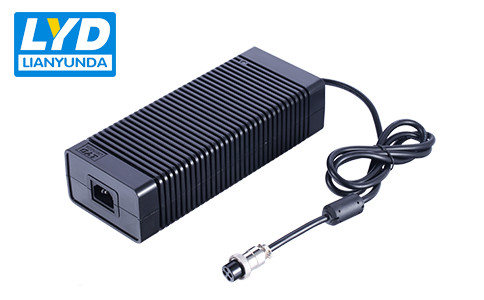
Main products: power adapter, medical power, LED power, charger and so on.
The excellent cost performance, perfect value, high-end quality, reliable performance, complete industry certification, strong company strength and professional service team can be purchased with confidence.
In the technology of developing IGBT, the power adapter is updated with the product, the manufacturing technology is continuously improved, and the fine processing is also possible. Now, the power device mainly adopts the processing size of 1 μm or less.
1 IGBT evolution from the first generation to the fourth generation, it is estimated that Uce (sat) can be reduced by 50%, tf can be increased by 50% to 60%, Table 22 lists the standard characteristics of each generation of power adapter Uce (sat) and tf.
2 Use a trench gate structure to reduce the chip size. In the process of development from the third generation to the fourth generation, the IGBT can make fine processing by forming a gate from the surface of the chip to the inside of the chip, because the gate is fabricated by digging a trench from the surface of the chip to the inside of the chip. Therefore, this structure is called a groove structure. Since the waist is grooved, the cell unit size is reduced to 1/5, the channel resistance of the MOSFET is lowered, the current density per unit chip area is increased, and the same rating can be manufactured. Power adapter with the smallest current and chip size.
3 Use new materials to improve product characteristics. One of the development trends of the next generation is to improve the characteristics of the power adapter by using a new material instead of Si. The second is to use the life time control method to locally create the window and reduce the dependence of Uce(sat) without increasing the Uce(sat). The switching characteristics are increased at speed; the third is to reduce the communication resistance of the MOs portion by means of fine processing. With these methods, the switching characteristics can be made the same as the MOSFET, so that the Uce (sat) and the thyristor are the same.